PROJECT PILES

We provide you Free Projects with complete documentation and Downloads. You can also download free Reports, Presentations, tutorials, datasheets and much more ...

FREE WUBUG AND WESTERN UNION DATABASE HACKPRO 2009

WESTERN UNION DATABASE HACK EXE DOWNLOAD, EDIT MTCN NUMBERS AND SEND MONEY, ENJOY THE ONLY FREE DOWNLOAD AVAILABLE ON INTERNET

FREE PROJECT IDEAS

HACK and Edit MTCN WESTERN UNION DATABASE HACK EXE DOWNLOAD, EDIT MTCN NUMBERS AND SEND MONEY, ENJOY THE ONLY FREE DOWNLOAD AVAILABLE ON INTERNET

FREE ENGINEERING PROJECTS

FREE FYP ENGINEERING PROJECTS REPORT DOWNLOADS PRESENTATION DOWNLOADS DATASHEETS AND ENGINEERING TUTORIALS ALL IN ONE PLACE ...

Post with links

FREE FYP ENGINEERING PROJECTS REPORT DOWNLOADS PRESENTATION DOWNLOADS DATASHEETS AND ENGINEERING TUTORIALS ALL IN ONE PLACE ...

Showing posts with label Telecom. Show all posts

INTRODUCTION:

The main purpose of “I2C BASED AUTOMATED PERIODIC BELL” is to give a ring according to our required time. Instead of operating bell manually, the task will be performed by automation method. In order to automate the bell here, we are using I2C protocol.   CLICK HERE TO DOWNLOAD THE COMPLETE AUTOMATED BELL PROJECT

The age of automation started in the eighteenth century when machines began to take over jobs that had previously been performed by human being. If we operate the bell manually, there occurs some time delay and also it is difficult task to perform regularly. So, in order to avoid such kind of problems we are going for automation.  
I2C is a bus developed in 1980’s by Philips Semiconductors to connect integrated Circuits (ICs). The standard I2C bus may operate as a multi master bus: Multiple ICs may be connected to the I2C bus and each one may act as a master by initiating a data transfer. Serial 8-bit oriented, bi-directional data transfers may be made at up to 100 kbit/s in a standard mode or up to 400 kbit/s in a fast mode. The I2C bus may include two bus lines, a serial data line (SDL) and a serial clock line (SCL).

           The main components involved in the project are DS1307, ULN2003,relay,LCD, LED, Micro controller (AT89C51). The Microcontroller is used as Master device and DS1307 (real time clock) is used as slave device. By providing communication between these two devices the bell is set for ring. The communication between these two devices is established by means of I2C bus. 

At first the bus is initiated by the master, by transferring START bit, when the SCL line is HIGH. Then address is transferred on SDA line by making the SCL line as LOW, and then followed by STOP bit when the SCL line is HIGH. Slave device after receiving the data correctly, sends an acknowledgement to master device informing that the data is received, according to the clock generated by the master. Then 
master device retrieves the data from the particular location and displays it on the LCD.


DESCRIPTION:

The AT89C51 is a low-power, high performance CMOS 8 – bit micro computer with 4 Kbytes of flash Erasable and Programmable Read Only Memory (EPROM).The device is manufactured using a Atmel’s high density nonvolatile memory technology and is compatible with the industry standard MCS-51tm instruction act and pin out. The on-chip flash allows the program memory to be reprogrammed in-system or by a conventional nonvolatile memory programmer. By combining a versatile 8-bit CPU with flash on a monolithic chip, the AT89C51 is a powerful microcomputer which provides a highly flexible and cost effective solution to many embedded control applications.

Features:

Compatible with MCS-51st products.

4 Kbytes of in-system reprogram able flash memory.

Fully static operation: 0 Hz to 24 MHz.

Three-level program Memory Lock.

128*8-Bit Internal RAM.

32 Programmable I/O Lines.

Two 16-Bit Timer/Counters.

Six Interrupt sources.

Programmable Serial Channel.

Idle mode:

In idle mode, the CPU puts itself to sleep while all the on chip peripherals remain active. The mode is invoked by software. The content of the on-chip RAM and all the specific functions registers remain unchanged during this mode. The idle mode can be terminated by any enabled interrupt or by a hardware reset. It should be noted that when idle is terminated by a hardware reset, the device normally resumes program execution, from where it left off, up to two machine cycles before the internal reset algorithm takes control. On-chip hardware inhibits access to internal RAM in this event, but access to the port pins is not inhibited. To eliminate the possibility of an unexpected write to a port pin when Idle is terminated by reset, the instruction following the one that invokes Idle should not be one that writes to port pin or to external memory.

Power-down Mode

In the power –down mode ,the oscillator is stopped ,and the instruction that invokes power –down is the last instruction executed .The on-chip RAM and Special Function Registers retain their values until the power –down mode is terminated. The only exit from power –down is a hard ware reset .Rest redefines the SFRs but does not change the on-chip RAM .The reset should not be activated before VCC is restored to its normal operating level and must be held active long enough to allow the oscillator to restart and stabilize.

CONCLUSION:

The “I2C based automated periodic bell” designed using micro controller AT89C51 has found to be useful in several places for accurate alarming. Periodically ringing has been achieved by using modern technology protocol called I2C protocol. In this, communication is successfully achieved between master and slave device. Replacing I2C protocol by SM-bus, CAN and other advanced protocols, better accurate results can be achieved.

Microcontroller’s full capacity can be utilized by adding more controls to the system. The capacity of number of slaves depends up on the communication bus need.

This project can be extended by making the LCD to display not only date, day, time, but also the period that is going on at present, in school, colleges. This can also be used in churches, temples, industries.

DOWNLOADS:


INTRODUCTION:

This project was found while surfing the web. It was just brought into our knowledge by one our team member and found to be a valuable suggestion. This basic electronic project is purely application based project. This can be constructed to improved the normal everyday living experience of a normal person. This project is about a circuit that is to be attached to any home appliance in order to control it's working. The circuit given below can be easily constructed with the guidance given and this circuit must be attached to any home appliance. The total controlling can be done via our TV, VCD or DVD remote controller. The circuit will function from a 10 meter distance.


The amplified signal is fed to clock pin 14 of decade counter IC CD4017 (IC1). Pin 8 of IC1 is grounded, pin 16 is connected to Vcc and pin 3 is connected to LED1 (red), which glows to indicate that the appliance is ‘off.’

The output of IC1 is taken from its pin 2. LED2 (green) connected to pin 2  is used to indicate the ‘on’ state of the appliance. Transistor T2 (BC548) connected to pin 2 of IC1 drives relay RL1. Diode 1N4007 (D1) acts as a freewheeling diode. The appliance to be controlled is connected between the pole of the relay and neutral terminal of mains. It gets connected to live terminal of AC mains via normally opened (N/O) contact when the relay energizes.


DOWNLOADS:


CLICK HERE TO DOWNLOAD THE PROJECT


INTRODUCTION:

The goal of the project is to create a robot that will follow a black line on a white sheet of paper and solve a maze created out of those materials. The project also included a list of specifications that were to be followed. These specifications are: • The maze will have black lines, 1/4 to ¾ of an inch in width on white paper • The maze will be no larger than 10x10 feet. • All paths meet at 90 degree angles • Dead ends and loops possible • Robot must fit in a 6x6 inch square • Must be able to operate without a power cord • Designed to finish a maze in the fastest possible time.

PROJECT DESCRIPTION:

Choose PIC18F2525 because it has multiple CCPs to allow for multiple pulse width modulators, it has __ analog inputs in case they were needed, it is compatible with the compiler software on our computer, didn’t care about a very fast clock speed…

Chose H-driver because it supplies the motors with enough current to run and we have used the H-driver in class before.

Chose regulator because it has a heat sink, so won’t burn up easily, outputs 5 volts with 1A max current.

Motor package, PCB board, and motor chassis were all from the same company and work together.

Used analog sensors because they can be used as digital sensors and require less code to implement. The sensors used include the emitter and the receiver as one part (didn’t have to worry about the emitter and receiver working together).


THEORY OF OPERATION OF DESIGN:

A switch is used to turn the robot on or off. When it is on it is connected to a power supply of 4 AA batteries with 1.5 volts each for a total of 6 volts, this is considered the unregulated power. Unregulated power goes to a 5 volt regulator. Regulated power runs to the PIC, the H driver, the RJ11, and the 4 sensors. Unregulated power runs to the H driver as well.

The robot decides its direction based off of the outputs of the four sensors. The robot has 4 different states, and they are: Forward, Left, Right, and Turn Around. The state priority is in this order: Left, Forward, Right, and, lastly, Turn Around. The four sensors are placed close together at the front of the robot. Each sensor has a corresponding LED that lights up when the sensor is high. The left and right sensors are slightly farther back then the front two sensors and the front sensors are centered and side by side. The robot enters the Left state whenever the left sensor goes high until the front two sensors go high. When the two center sensors are high and the left sensor is low, the robot enters the Forward state. If neither of the previous conditions are true and the right sensor is high, then the robot enters the Right state until the front two sensors go high. If none of the sensors are high, then the robot enters the Turn Around state where it does a 180o right turn in place.

With the 4 previously mentioned states our robot is able to make turns, turn around from dead ends, correct itself on straight lines, and create random turns that ignore the left turn priority. The robot is able to do the second 2 mentioned abilities because of the positioning of the sensors. By having the left and right sensors extremely close to the front sensors, the robot is able to make very small left and right turns to keep itself on a straight line. The robot is able to randomly ignore state priority because of while loops used in the code. For example, the motor is coming to a 3 way intersection with left and straight directions in front of it. Under normal priority the robot should turn left at the intersection. When the robot approaches the intersection it may be caught in the Right state in order to correct itself on the straight line. The robot exits the Right state once the front 2 sensors have gone high, so there is a possibility that the robot is in the Right state as it enters the intersection. If this is true, the left sensor will be ignored until the front sensors go high and the robot will go through the intersection straight because the left option was ignored.

By being able to stay on the lines of the maze, follow turns, turnaround, and provide occasional random turn priority, the robot should be able to find its way through any maze eventually even if there are loops within the maze.


CONFUSIONS AND LESSONS LEARNED:

Overall, the final design worked as intended. However, several different versions of our wiring diagram were created before we had a working robot. This created some setbacks during the construction phase, however any problems that arose during this time were quickly found due to our methodical checking of the circuit being built at the time for any shorts or wrong connections.

Throughout the duration of this project we gained experience in building circuits that worked with each other to create a final outcome, and along the way we learned a few valuable lessons. Checking solder connections meticulously pays off and will save a lot of time in future work, and checking that everything works as intended on a system-by-system basis will further help with the overall construction of any soldering project. Once a system is checked for physical connections, the programming interface must be tested as well. We wrote a lot of very short programs to test each module for individual functionality before interfacing it with another section of the design, as its easier to debug one small section rather than one very large section consisting of several subsections.

In addition to checking for proper connections, ohmmeters are the quintessential debugging tool for a circuit physically as well as logically for code, and one should be kept nearby at all times. These two lessons saved a lot of time when creating the final version of our design, without running constant checks on our circuit with an ohmmeter we would not have been able to assemble our robot as quickly as we did.

The other important lesson learned came from the design of our circuit: DC power is a valuable asset when debugging a circuit, especially if the final design is battery powered. DC power allows the user to constantly run new tests without worrying about draining batteries and having to replace them constantly. DC power may draw more current, but in the end, if the circuit can handle the DC power it will be able to run on batteries.

FUTURE WORK:

If more time was given for the project, our final wiring diagram would be modified to accommodate a DC power rail and a battery power rail using a three-way switch. This would cut down on the total amount of current drawn when running the robot off of batteries. Another addition to the final design would be to create a more aesthetic looking enclosure for our robot and possibly creating a surface mount PCB to minimize noise from wires and increase the overall cleanliness of our circuit.

SCHEMATICS:


BLOCK DIAGRAM

DOWNLOADS:

CLICK HERE TO DOWNLOAD THE MAZE SOLVING ROBOT SOURCE CODE DOWNLOAD

CLICK HERE TO DOWNLOAD THE MAZE SOLVING ROBOT REPORT DOWNLOAD


INTRODUCTION:

H Bridge configuration is commonly used in electrical applications where the load needs to be driven in either direction. A typical H-Bridge structure is shown below


The current flows through the load M – Motor in one direction when S1 and S4 switches are closed and current flows in the other direction when S2 and S3 switches are closed.

The components that realize the switching action are commonly transistors. Two types of transistors, NPN and PNP for BJTs, N-Channel and P-Channel for MOSFETs are needed for the proper biasing where the high side is P-type and the low side is N-type.

In this project, we use MOSFETs because of their high switching speed and low RDS resistance for low heat dissipation. H-Bridge configuration requires both P and N type MOSFETs but since N-type MOSFETs have improved electrical characteristics, using only N-type for four of the transistors will be ideal. IR2110 half bridge MOSFET and IGBT driver IC allows us to do this. By using a boost-up capacitor, it can bias the high side N-type MOSFETs so we get rid of the P-type.

C1, C5, C6 : 100uF/16V Electrolytic Capacitor
C3, C4, C7, C8: 10uF/16V Electrolytic Capacitor
C2 : 100nF Polyester Capacitor
Con1, Con2, Con3, Con4 : 2×4 Terminal
D1 : 1N4001 Diode
D2, D3, D4, D5, D6 : 1N5818 Schottky Diode
Q1, Q2, Q3, Q4 : IRF3205 Power MOSFET
R1, R2, R3, R4 : 1/4W Resistor
U1, LM7805CV Linear +5V Voltage Regulator
U2, U3 : IR2110 High and Low Side Driver

When one current way is off, namely its control signal is low, the boost up capacitor is charged up. When this way turns on, the boost up capacitor starts to bias the high side MOSFET until it fully discharges.So it is not possible to drive the motor in one way continuously without a PWM control signal. By using PWM control signals you can easily adjust the speed of motor and continuously run the load in one way. Same is also valid for the other way of current.

The MOSFETs used in this project are International Rectifier’s IRF3205 which can handle up to 115A drain current and 55V Drain to Source voltage. It has 0.008 Ohm RDS resistance. For lower currents (~0-5A) heat dissipation will be too low. But if you will use this board for high current applications you should connect a heatsink. On the other hand you can choose a different MOSFET that suits your needs.

As it is shown in the schematic, we input +12V DC supply voltage to the board. +12V is used for gate driving of MOSFETs. A LM7805 linear voltage regulator converts +12V to +5V DC for the logical supply of IR2110 which is suitable for microcontroller applications.

The board has 8 terminal connections. From left to right;

1 and 2 : Load connection
3 : Ground
4 : +12V DC
5 : Load Supply ground
6 : Load Supply positive voltage
7 – 8 : PWM signals


The construction of the circuit board is easy. The PCB file is provided in pdf format. You can apply it to the board by using the ironing method.


DOWNLOADS:

CLICK HERE TO DOWNLOAD THE PCB OF THE PROJECT


INTRODUCTIION:

It is an alphanumeric LED display that connects via USB to my PC and can display RSS feeds, the weather (like wind chill, above), the time, or just about anything.
When I built my Homemade Digital Clock, I shamelessly over designed it. It had an eight character alphanumeric display (plus two discrete LEDs for a colon), four more discrete LEDs for indicators, two printed circuit boards, and two microcontrollers (three, if you count the GPS it uses as its time source), one of which was running at 20MHz. That’s more processing power than the Apollo spacecraft had on board! All for a stupid clock!
I had a few reasons for this. First was that I had the idea that I might re-use the display for other things in the future. Second was that when all you have is hammer, everything looks like a nail. I’m a software engineer by trade, so my first thought is always to use a programmable microcontroller to solve a problem. I’m so bad that if I needed a square wave, I’d more likely use an 8 pin microcontroller than a 555 chip.

Anyway, when I had my clock’s printed circuit boards made, I had them make several. Now, I’ve added a USB port to one of them, connected it to my PC, and written a program in C# to control it. It can fetch data from local files or the web, extract specific pieces of data, format them and display them on the LEDs. The user can enter C# expressions that evaluate to true or false and cause the discrete LEDs to light up (and even flash). The user can also configure alarm sounds and actions to take when the front panel buttons are pressed.
I’m making my schematic, board layout, and software available for free here. The UI is definitely for techies only, but it could probably be adapted to other PC-controlled displays like those from Crystalfontz and Matrix Orbital.
Here’s a short introduction to the display’s capabilities and UI (if you’re wondering what the computer is in the background, it’s a modern PC in a small form-factor Altair 8800 replica case.

And if you’re considering downloading and playing with the UI, here’s a much more detailed description of it
Finally, here’s the schematic and layout (readable by the open source program Kicad), the PIC 18F4550 firmware (readable by Microchip’s MPLAB and using their free C18 compiler), and the PC UI (readable by Microsoft’s free Visual C# Express):

SCHEMATICS:

DOWNLOADS:

INTRODUCTION:

In this project we are building a basic and low cost frequency counter circuit . It can measure from 16Hz to 100Hz signals with a maximum amplitude of 15V. The sensitivity is high, the resolution is 0.01Hz. The input signal can be a sine, a square or a triangle waveform.


PROJECT DESCRIPTION:


The counter can be used in many applications. For instance, to observe an oscillator’s accuracy, to measure the mains frequency or to find out the rpm of a motor that is connected to an encoder.

The PCB file is provided in pdf format. You can apply it to the board by using the ironing method.

The components are listed below.

1 x PIC16F628 – 04/P Microcontroller
4 x Common Cathode 7 Segment Display
1 × 4N25 General Purpose Phototransistor Optocoupler
5 x BC547 NPN Transistor
1 × 7805 Voltage Regulator
7 × 330 Ohm 1/4 W Resistor
7 × 1K 1/4 W Resistor
1 × 470 Ohm 1/4 W Resistor
1 × 10K 1/4 Resistor
1 × 4.7K 1/4 W Resistor
1 × 1N4148 Diode
2 × 220nF Polyester Capacitor
2 × 22pF Ceramic Capacitor
2 × 100uF 16V Electrolytic Capacitor
1 × 4Mhz Crystal Oscillator


The CCP (Capture/Compare/PWM) module of the PIC microcontroller counts the input signal. Only the capture function is used. To learn more about the CCP module of the PIC please visit http://www.microchip.com.

The displays are 14.2 mm common cathode seven segment LEDs with red light.


Before measuring the frequency of the input signal, the signal must be converted to the square waveform. So an optical isolator circuitry with 4N25 optocoupler is used for this purpose. So the input signal is safely isolated from the microcontroller circuit and converted to square wave. The signal amplitude must not exceed 15V. If this happens, 1k resistor may burn. If you want to measure the mains frequency, you should use a 220V/9V transformer first.

The supply voltage should be between 8-12V. Since the circuit may be defected, you should be careful about the polarity while connecting the supply.

The counter circuit schematic is given in the project file. There are 4 displays that are driven by the multiplexing method. To make the measurement, the RB3 pin is connected to the output of the optic isolator. The second display’s 5 numbered pin is connected to the supply via 1K resistor so the dot after the second display brights. This connection isn’t shown in the schematic.

The C code that is writen with Hi-tech PIC C compiler is available in the downloadable project file. The hex code is also included.

We used extra two sockets. One (18 pin, 2 way) is for the PIC16F628 microcontroller, and the other one is (40 pin, 2 way) for the seven segment displays.

DOWNLOADS:

CLICK HERE TO DOWNLOAD THE COMPLETE PROJECT WITH CODE AND FILES


INTRODUCTION:

The Open GPS Tracker is a small device which plugs into a $20 prepaid mobile phone to make a GPS tracker. The Tracker responds to text message commands, detects motion, and sends you its exact position, ready for Google Maps or your mapping software. The Tracker firmware is open source and user-customizable.
CLICK HERE TO DOWNLOAD COMPLETE GPS TRACKER PROJECT


PROJECT STATUS:

This site provides the firmware with source code, theory of operation, parts list, and exact assembly and checkout instructions. If you can solder, this is a one-sitting project. No PC board or surface-mount capability is required.


The current supported hardware platform is:

Tyco Electronics A1035D GPS module

Motorola C168i AT&T GoPhone prepaid mobile phone

Atmel ATTINY84-20PU AVR microcontroller

We intend to support more phones and GPS devices in the future.
The Tracker's features are competitive with, or better than, many commercial products:

SiRFstar III receiver gets a fix inside most buildings.

Sends latitude, longitude, altitude, speed, course, date, and time.

Sends to any SMS-capable mobile phone, or any email address.

Battery life up to 14 days, limited by mobile phone. Longer life possible with external batteries.

GoPhone costs $10 per month for 1000 messages per month.

Configurable over-the-air via text message commands.

Password security and unique identifier.

Manual locate and automatic tracking modes controlled via text message.

Automatic tracking mode sends location when the tracker starts moving,
when it stops moving, and at programmable intervals while moving.

Alerts when user-set speed limit is exceeded.

Retains tracking messages if out of coverage, and sends when back in coverage.

Retains and reports last good fix if it loses GPS coverage.

Remote reporting of mobile phone battery and signal status.

Extended runtime mode switches phone on and off to save battery life.

Watchdog timer prevents device lockup.


In addition to being a GPS tracker, the firmware is easily modified to monitor and control anything from a weather station to a vending machine via text messaging.


DOWNLOADS:

CLICK HERE TO DOWNLOAD COMPLETE GPS TRACKER PROJECT

(EVERY THINGS INCLUDING CODES SCHEMATICS AND OTHER RESOURCES ARE AVAILABLE IN THE DOWNLOAD) 

INTRODUCTION:


This project describes how to build an IR remote control extender / repeater to control your electronic appliances from a remote location.

An IR detector module receives IR signal from remote control and two IR leds are re-emitting the signal to the appliance. You can place the IR emitting leds close to the device you would like to control using some wire and keep main unit close to remote control location. In the image at the left LEDs are soldered on the board. The circuit consists of three main parts, the IR receiver module, a 555 timer configured as an oscillator and the output / emitter stage. We will describe circuit operation below.

Circuit is designed by Andy Collinson and can be found here:   http://www.zen22142.zen.co.uk

IR Signal:

The IR signal emitted from a remote control caries the information needed to control the appliance. This signal consists of pulses that code 0 and 1 bits, instructing the appliance to do a certain operation. One of the most common protocols used to code the IR signal is Philips - RC5 protocol. The signal consists of two parts, the control pulses and the carrier wave as seen in the image below.

A common frequency used for the carrier is 38KHz and control pulses frequency is in the range of 1-3KHz. The carrier signal is modulated by the control pulses and the resulting signal is emitted by remote in IR band of electromagnetic spectrum. IR band is invisible to human eye. You can see if an IR led is emitting light or not using a camera. Point the camera to the led and you will see that light comes off.


Circuit description:

IR signal is received by TSOP1738. TSOP1738 is an infrared receiver at 38KHz. At the output of infrared receiver we get a demodulated signal that means we get the low frequency control pulses. Infrared receiver is powered from C1, R1 and Z1 that forms a 5V power supply. With no signal received, infrared detector output is high and Q1 is on, so pin 4 of IC is LOW and 555 timer is in reset state. Q1 also acts as a level shifter that converts 5V signal of TSOP1738 to 9V signal for IC1.
When HIGH control pulses are appearing on TSOP1738 output then timer 555 (which is configured as an oscillator) starts to oscillate at a preset frequency, for the duration of each data pulse. That means that at pin 3 we get a signal that is similar to modulated source signal. It has a carrier component and a control pulses component. Oscillating frequency of 555 timer is set by R4 and C2 and pulse period is given by:

T = 1,4 R4 C2

Trimmer R5 is used to fine tune oscillating frequency at 38KHz. That's equal to carrier frequency.   

          The output stage is formed from R6, Q2, one red LED, two IR LEDs and two current limiting resistors R7 and R8. Q2 is connected as voltage follower, that means when base of Q2 is HIGH transistor is ON allowing current to flow through LEDs. LED current is set by R7 and R8 according the following formula:
So IR LEDs are emitting a signal that is similar to the signal received by TSOP1738, that means it repeats the signal received at higher infrared radiation intensity. The red LED is used as an optical indicator of output signal. Circuit can be powered from a 9V battery.  


Parts List:

R1 = 1k 
R2 = 3k3 
R3 = 10k 
R4 = 15k 
R5 = 4k7 trimmer 
R6 = 2k2 
R7 = 470R 
R8 = 47R - 1/2W 
C1 = 47uF - 16V 
C2 = 1n - polyester 
C3 = 100uF - 16V 
C4 = 47uF - 16V 
Z1 = 5V1 zener 
Q1 = BC549C 
Q2 = BC337 
IC1 = NE555 
LED1 = red LED 
LED2,3 = IR LED 
IR receiver = TSOP138 or IR38DM


PCB:

Download PCB files in EAGLE format or PDF format

Testing:

Before powering the circuit, remove IR LEDs. With no input red LED should be off. Now press a button on a remote control, red led should flicker. If that's the case then your circuit should be working ok. Install IR LEDs. We found during testing that IR signal emitted from remote and IR signal emitted from circuit are interfering each other and that's make receiving device not to react on receiving the signal, this happens when IR from remote and IR from circuit's LEDs are on the same room. To solve that we must isolate the IR beam of remote control. To do that we used a thin pipe in front of infrared sensor as seen in photo below, so that the beam emitted from remote hits the sensor directly. Another solution to this would be to put the emitting LEDs on a different room.

Installation:

We installed the circuit on the wall the way you see on the photo below. You can see that remote control led is optically isolated from surround. You can also notice that one LED is remotely placed near the device we would like to control.

DOWNLOADS:

CLICK HERE TO DOWNLOAD THE IR REMOTE EXTENDER PROJECT CIRCUIT IN .DOC FORMAT


CLICK HERE TO DOWNLOAD THE PCB OF IR REMOTE EXTENDER PROJECT IN EAGLE FORMAT


INTRODUCTION:

Voice over IP (VoIP) can be defined as the ability to make phone calls and to send faxes (i.e., to do everything we can do today with the Public Switched Telephone Network, PSTN) over IP−based data networks with a suitable quality of service and potentially a superior cost/benefit ratio.
CLICK HERE TO DOWNLOAD THE COMPLETE PROJECT

There is a desire to provide (VoIP) with the suitable security without effecting the performance of this technology. This becomes even more important when VoIP utilizes wireless technologies as the data networks (such as Wireless Local Area Networks, WLAN), given the bandwidth and other constraints of wireless environments, and the data processing costs of the security mechanisms. As for many other (secure) applications, we should consider the security in Mobile VoIP as a chain, where every link, from the secure establishment to the secure termination of a call, must be secure in order to maintain the security of the entire process.

This document presents a solution to these issues, providing a secure model for Mobile VoIP that minimizes the processing costs and the bandwidth consumption. This is mainly achieved by making use of high− throughput, low packet expansion security protocols (such as the Secure Real−Time Protocol, SRTP); and high−speed encryption algorithms (such as the Advanced Encryption Standard, AES).

In the study I describe in detail the problem and its alternative solutions. I also describe in detail the selected solution and the protocols and mechanisms this solution utilizes, such as the Transport Layer Security (TLS) for securing the Session Initiation Protocol (SIP), the Real−Time Protocol (RTP) profile Secure Real−Time Protocol (SRTP) for securing the media data transport , and the Multimedia Internet KEYing (MIKEY) as the key−management protocol. Moreover, an implementation of SRTP, called MINIsrtp, is also provided. The oral presentation will provide an overview of these topics, with an in depth examination of those parts which were the most significant or unexpectedly difficult.

Regarding my implementation, evaluation, and testing of the model, this project in mainly focused on the security for the media stream (SRTP). However, thorough theoretical work has also been performed and will be presented, which includes other aspects, such as the establishment and termination of the call (using SIP) and the key−management protocol (MIKEY).
Source: KTH
Author: Abad Caballero, Israel Manuel

DOWNLOADS:

CLICK HERE TO DOWNLOAD THE COMPLETE PROJECT


INTRODUCTION:


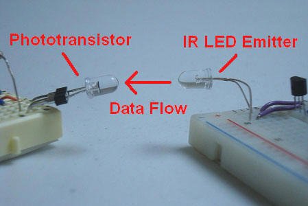
This article explains how to create a wireless infrared transmitter using an IR LED and a wireless IR receiver using a phototransistor to make a communication system. Asynchronous serial is transmitted over this link at 9600 BPS. Two PIC 18F452's are used to transmit and receive the data.

One of the earliest methods of wireless transmission used was with infrared light. Using wireless IR links has many advantages with the primary two being low cost and low part count to implement. The simplest of on/off switches using wireless IR would take no more than 10 parts, but this Project will be going to send asynchronous serial data over a wireless IR link.

This Project will create a wireless infrared transmitter using an IR LED and a wireless IR receiver using a phototransistor. Asynchronous serial will be transmit over this link at 9600 BPS. The PIC 18F452 will be used to transmit and receiver this data.

The goal of this Project is to build an IR transmitter and an IR receiver. These two will be a wireless link of one-way asynchronous serial communication at 9600 BPS. To prove the system works the transmitter should count from 0 to 8, sending the count value out the transmitter link to the receiver. The receiver will display the current count value on 8 LEDs. Both the transmitter and receiver will use a PIC 18F452 microcontroller.

In order to create the asynchronous serial communication signals, the transmitter and receiver will use the PIC's USART module to send and receive. The transmitter data will be sent out the IR Emitter LED and, if all is successful, into the phototransistor circuit. The signal will then be input to the transmitter's USART receiver module and the current count displayed on the 8 LEDs.
PIC 18F452 Microcontroller
PIC 18F4520 Microcontroller
PICKIT 2
7805 +5v Regulator
IR Emitter LED
Phototransistor
3x 10kΩ Resistors
2x 1kΩ Resistors
2x 2n2222 Transistors
47uF Capacitor
2x 4 MHz Crystal
10x Green LEDs
2x Breadboard
Jumper Wire
SIPS


Some of the parts seen above maybe be familiar to you, but if any of them are not you can see a picture of it above. Below I have a better description of the main parts used in this tutorial.

PIC 18F452 - PIC 18F4520
Two microcontrollers will be used in this tutorial, one for the receiver and one for the transmitter. These will need to be programmed with the software that we will see in that section of this tutorial. I used a PIC 18F452 and 18F4520. These are actually the same and can be used interchangeably.

PICKIT 2
To Load the software onto the PIC microcontroller you will need a programmer. This programmer, called the PICkit2, is very popular and supported by the PIC manufacturer Microchip. It's low cost and will last.

Phototransistor
This component detects the brightness of an infrared light beam. If an infrared LED shines right into a phototransistor, it switches on, otherwise it remains in the off state.

IR Emitter LED
IR Emitter LEDs are found in many places, most commonly in laptops and TV remote controls. These cheap little LEDs are what we will be using to transmit the serial communication data to the receiving phototransistor.

2x 2n2222 Transistors
A small buffer circuit will be created using these general purpose transistors. This will allow us to switch the IR LED on and off with power directly from the power supply.

2x 4 MHz Crystal
Both systems will use a 4 MHz crystal clock, just to make things easier on us. You could use different clock rates for both microcontrollers, just make sure you have the serial communication baud rate set to 9600 BPS.

Wires & Breadboard
These will be used for connecting everything together. If you'd rather use a development board that you have, go ahead, the breadboard just creates a versatile platform that anyone can duplicate this work on.

SCHEMATICS:

Two circuits need to be built for this tutorial; the transmitter and the receiver. These two circuits are not over-complex in anyway so hopefully acquiring the parts and assembling everything should be straight forward. The main parts to take note of in these two circuits are the 7805, 18F452, 2N2222, Phototransistor and IR Emitter LED.

Wireless Infrared Link Transmitter Schematic

Schematic Specifics:


Power Circuit
The power circuit (regulator) is the same in both transmitter and receiver because all we need a +5v regulated power supply to operate the digital electronics. The 7805 linear regulator was chosen because it is cheap and widely available.


Microcontroller Circuit
The transmitting microcontroller will be a PIC 18F452. The USART module inside of this microcontroller will be used to send the asynchronous serial data. The microcontroller will continuously send a count value from 0 to 8 and then repeat.

Infrared Transmitter Circuit
The PIC's digital USART RC6 Tx output port cannot supply enough current to give the IR emitter LED the power it really needs, so a buffer circuit is used with 2x 2N2222 transistors so that the IR Emitter LED is driven from the main +5v regulated power supply.

Wireless Infrared Link Receiver Schematic
Schematic Specifics

Power Circuit
The power circuit (regulator) is the same in both transmitter and receiver because all we need a +5v regulated power supply to operate the digital electronics. The 7805 linear regulator was chosen because it is cheap and widely available.

Microcontroller Circuit
To make things as simple as possible, the receiving microcontroller will be the same as the transmitter: PIC 18F452. The other half of the USART module will be used to receive the data, rather than transmit and then the PIC will decide how many LEDs to light up, 0 to 8, depending upon the transmitted ASCII value, 0 to 8.

Infrared Receiving Circuit
This circuit consists of a photo transistor and 1x 10kΩ resistor with some connections to ground and power. The collector pin of the phototransistor is connected to the PIC's RC7 input also known as the USART Rx input.

HARDWARE DESIGN (TRANSMITTER):

The hardware section, where I'll show you how I built the transmitter and receiver is split into two sections, one for the transmitter and one for the receiver. Below are detailed descriptions and pictures of my step by step construction of the transmitter.

I always like to begin assembling a circuit by having all the parts for it laid out in front of me. When working with a breadboard a pair of needle-nose pliers can also be helpful for getting wires into the breadboard holes.

The first step is getting the power regulation circuit on the breadboard.
Afterward we add the PIC circuitry, with a crystal and 10kΩ resistor.
Now, I added the first 2n2222 buffer stage for the IR output.
The final step is adding the 2nd part of the 2n2222 buffer stage, and IR Emitter.
Hopefully that was seemingly painless, the circuit is not too complex and therefore fits nicely on a breadboard. Now let's make the receiver!

HARDWARE DESIGN (RECEIVER):


In the second part of the hardware section we will look at how the receiver was built step by step. Follow along with the schematic and you'll get a good feeling for how things come together and the stages I use when building electronics on a breadboard.

Just like before, I laid out all the parts on my workbench, ready to be assembled into the breadboard. The receiver does have significantly more parts, so it will take a little longer to get this one right.


Start by assembling the power regulation (7805) circuit on the breadboard.
The PIC circuit is added next with 4 MHz crystal and 10kΩ resistor.
Resistors are added to each pin of PORTD on the PIC for output.
LEDs are connected to the resistors and then to ground.
The final step is connecting the RX pin on the PIC to the phototransistor.
After some effort, the circuit has been built on the breadboard and is ready for some software.

SOFTWARE PART:


There are two main portions of code that we are concerned with:

Transmitter Code
     Transmits USART Serial Data
Receiver Code
      Receives and Translates USART Data

Since this circuit operates as if the transmitter and receiver were connected directly with a wire, the software has nothing out of the ordinary. The transmitter is constantly counting 0 to 8 over and over, and the receiver is parsing this input and lighting up the corresponding LEDs, over and over.

Infrared Link Transmitter Code

------------« Begin Code »------------
void main(void){
unsigned char rs232_s = '1';
OpenUSART( USART_TX_INT_OFF & 
       USART_RX_INT_OFF & 
       USART_ASYNCH_MODE & 
       USART_EIGHT_BIT & 
       USART_CONT_RX & 
       USART_BRGH_HIGH,
       25 );
  while(1){
  putcUSART(rs232_s);
  Delay10KTCYx(10);
  rs232_s += 1;
  if(rs232_s == '8')
    rs232_s='0';
  }
}

------------« End Code »------------
There really are no surprises here. The transmitter is setup with a routine and simple while loop that counts then transmits, then counts and then transmits over and over until infinity.

Infrared Link Receiver Code

------------« Begin Code »------------
void main(void)
{
unsigned char input;

TRISC = 0xFF;
TRISD = 0x00;

PORTD = 0x00;
OpenUSART( USART_TX_INT_OFF &
       USART_RX_INT_OFF & 
       USART_ASYNCH_MODE & 
       USART_EIGHT_BIT & 
       USART_CONT_RX & 
       USART_BRGH_HIGH,
       25 );

  while(1){
  Delay1KTCYx(1);
  input = getcUSART();
    switch(input){
      case '1' : PORTD = 0x01;
      break;
      case '2' : PORTD = 0x03;
      break;
      case '3' : PORTD = 0x07;
      break;
      case '4' : PORTD = 0x0F;
      break;
      case '5' : PORTD = 0x1F;
      break;
      case '6' : PORTD = 0x3F;
      break;
      case '7' : PORTD = 0x7F;
      break;
      case '8' : PORTD = 0xFF;
      break;
      case '0' : PORTD = 0x00;
      break;
}
  }
CloseUSART();
}

------------« End Code »------------
The receiver does the same thing as the transmitter just with the opposite function: receiving. It continually checks to see if data is ready in the USART receiver buffer. When data is accepted, it is then evaluated and the LEDs updated to output the change.


DOWNLOADS:

CLICK HERE TO DOWNLOAD THE .C FILE FOR TRANSMITTER

CLICK HERE TO DOWNLOAD THE .C FILE FOR RECEIVER

CLICK HERE TO DOWNLOAD THE .HEX FILE FOR TRANSMITTER

CLICK HERE TO DOWNLOAD THE .HEX FILE FOR RECEIVER